Nano Image Award
Nano Image Award 2025

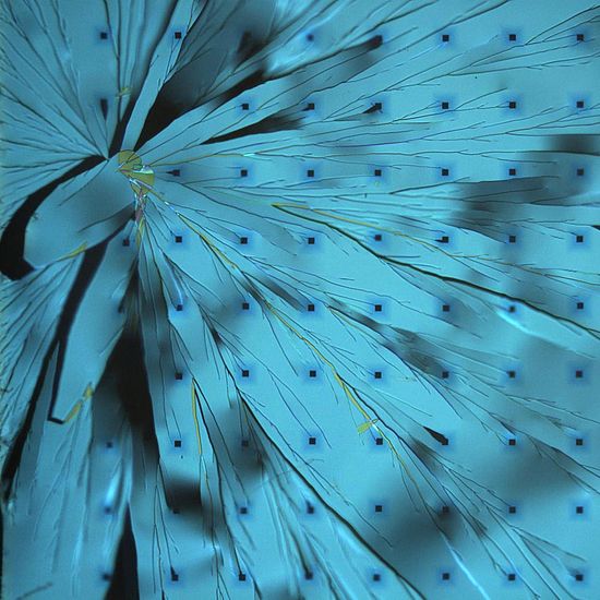
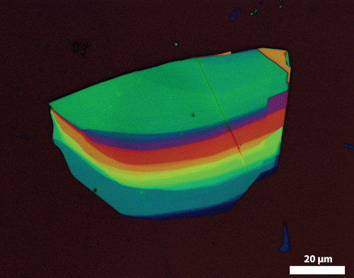
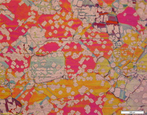
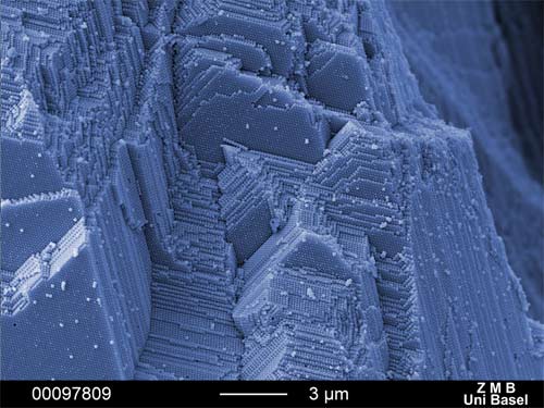
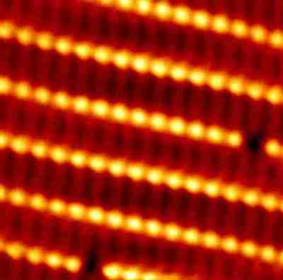
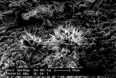
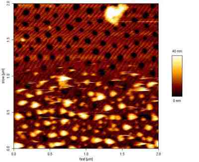
Ein einzelnes Wolframdiselenid-Dreieck auf Graphen/ Siliziumkarbid (SiC) zerfällt in Dreiecke innerhalb von Dreiecken und es bilden sich verschachtelten Facetten. Die AFM-Höhenkarte (Tapping-Modus) zeigt das Muster, und die diagonalen Bänder zeichnen die SiC-Stufenterrassen nach, die das Wachstum leiten. Ángel Labordet (Empa und SNI, Universität Basel)
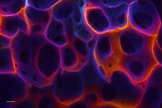
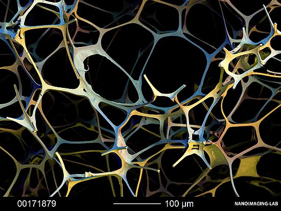
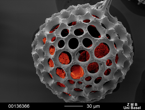
Die offenporige Struktur besteht aus natürlichem Albumin und bildet ein stabiles, biokompatibles Proteinnetzwerk. Ihre hochgradig vernetzte Porenstruktur bietet eine optimale Mikroumgebung für die Zelladhäsion und Gewebeintegration, was sie zu einem vielversprechenden Gerüst für die Knochen- und Knorpelregeneration macht. (Massstab: 100 µm) Sven Zaugg (FHNW und Univerität Basel)


Nano Image Award 2023

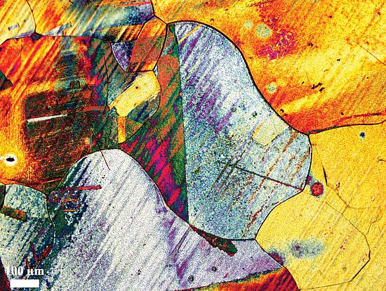
Ein Röntgenkondensator, aufgenommen unter einem Lichtmikroskop. Seine komplizierte Geometrie beugt das sichtbare Licht und macht ein Spektrum leuchtender Farben sichtbar, wobei jeder Farbton für eine bestimmte Wellenlänge steht. Der Durchmesser des Kondensators beträgt 2 mm, die geringste Linienbreite 50 nm. Das Gerät wurde für das Röntgenmikroskop des Forschungszentrums Hereon in Deutschland entwickelt. Peng Qi, Joan Vila-Comamala, Di Qu Paul Scherrer Institut

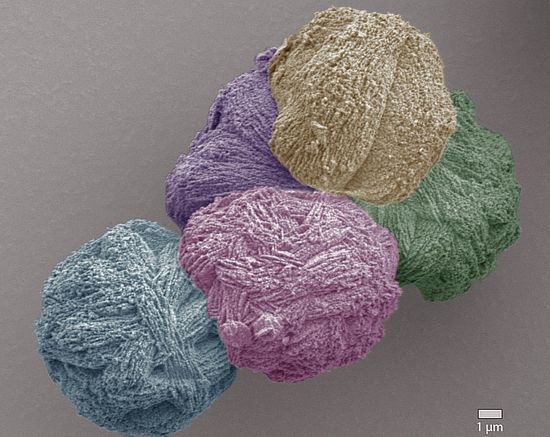
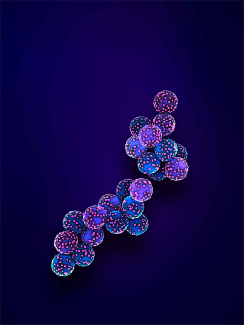
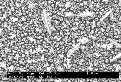
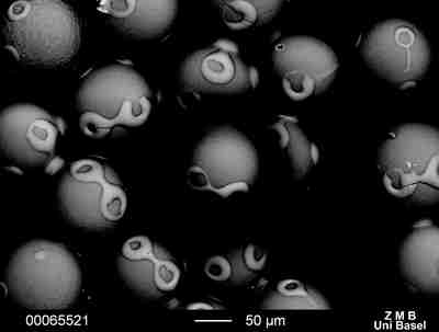
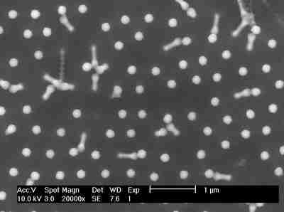
Die Mikrokugeln wurden aus Styrol durch mulsionspolymerisation von Studierenden im Praktikum Polymere an der FHNW hergestellt. Die Kugeln bilden beim Trocknen auf dem Probenhalter ein hexagonal geordnetes Gebilde. Das Bild wurde mit einem Elektronenmikroskop aufgenommen. Die Kugeln sind ursprünglich weiss, das Bild wurde mit Adobe Photoshop eingefärbt. Vivien Hollenstein, Laura Martinez und Sina Saxer FHNW Hochschule für Life Sciences

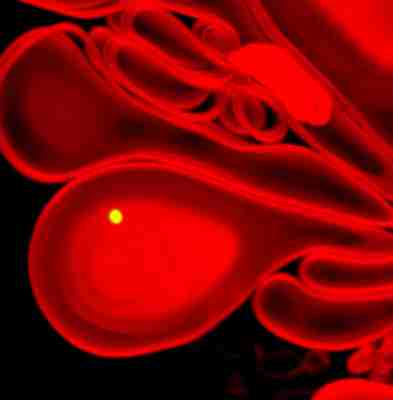
Ansicht der Mittelhirnregion einer Zebrafischlarve unter dem konfokalen Mikroskop. Die Endothelzellen des Gefässsystems, welche die Blut-Hirn-Schranke bilden, werden sichtbar (grün). Rot fluoreszierende Tracer, die das grüne Gefässsystem verlassen, zeigen an, dass die Blut-Hirn-Schranke in Gegenwart von toxischen Substanzen undicht wird. Ramya Deepthi Puligilla Departement Pharmazeutische Wissenschaften, Universität Basel


Nano Image Award 2022
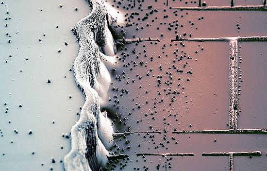
Farbkristall-Orientierungskarte eines 3D-gedruckten (additiv hergestellten) Edelstahls nach dem Ätzen der Oberfläche, um die SPuren des Schmelzbades sichtbar zu machen. Das Material ist porös (schwarze runde Kreise an den Spitzen der Schmelzbadspuren sind die Poren), wodurch das Wachstum der Kristallite im Material während der Erstarrung unterbrochen wird. Daher besteht jedes Schmelzbad aus mehreren kleinen Kristalliten mit unterschiedlicher Ausrichtung. Dr. Efthymios Polatidis und Christos Sofras Laboratory for Neutron Scattering and Imaging (LNS), Paul Scherrer Institute
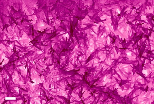
Gewachsene Kristalle aus Fluorapatit auf einer behandelten Zahnoberfläche. Das Bild wurde in Vorbereitung auf eine Veröffentlichung gemacht, die auch Ergebnisse aus dem Nano-Argovia-Project Nanocure enthält. Dr. Lucy Kind FHNW School of Life Sciences, Muttenz
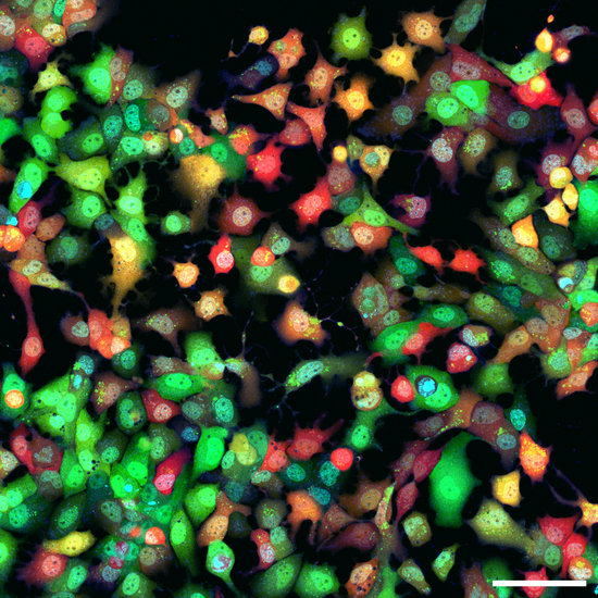
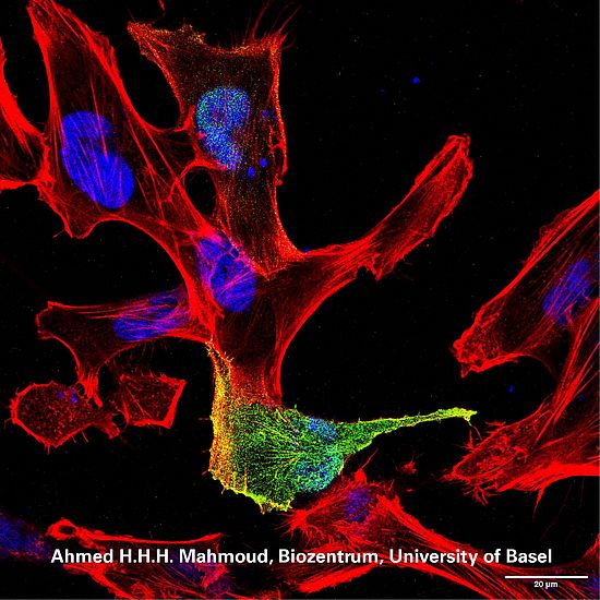
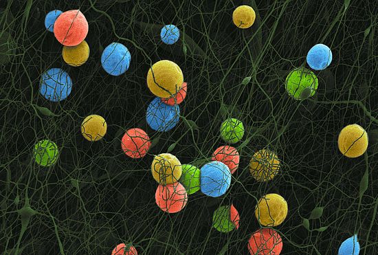
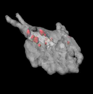
Analyse von menschlichen Zellen, die ein fluoreszierendes Protein nach einem Gentransfer exprimieren. Lipid-Nanopartikel (LNP) wurden dabei als Träger für genetisches Material verwendet. Gezeigt ist eine Analyse der Zellen mittels konfokaler Mikroskopie. Hellgrüne Flecken: endosomale Freisetzung, grünes Signal: Galectin3-GFP, rotes Signal: Transgen RFP, cyanfarbenes Signal: Zellkerne, blaues Signal: LNP Claudio Alter, SNI-Doktorandenschule, Departement für Pharmazeutische Wissenschaften, Universität Basel


Nano Image Award 2021
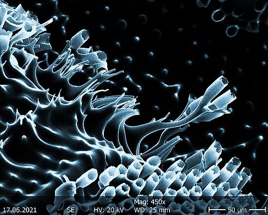
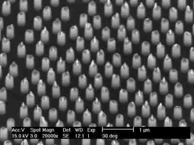
Christmas candles - Scanning electron microscopy image of artifact structures on a hot-embossed polymer film Manuel Kraus (CSEM Center Muttenz)


Nano Image Award 2020
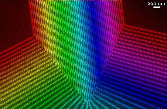
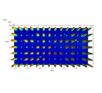
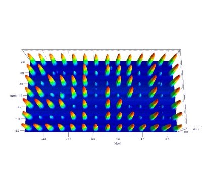
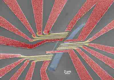
Gate Array Rasterelektronenmikroskopische Aufnahme von Teilen einer Spin-Qubit-Vorrichtung, die durch Elektronenstrahl-Litho- graphie hergestellt wurde. Sie ist in Regenbogenfarben eingefärbt, weil sich die Strukturen in einem Abstand, der etwas kleiner als die Wellenlänge des sichtbaren Lichts ist, anordnen und sich daher je nach Betrachtungswinkel in unterschiedlichen Farben zeigen. Jann Hinnerk Ungerer SNI PhD Student Departement Physik, Universität of Basel
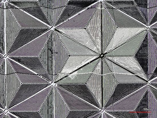
INKA Maske Konfokales Laser-Scanning-Mikroskopie-Bild eines Lacks auf einer PET-Folie, abgeformt von einer laserstrukturierten Stahlvorlage Maßstab: 280 µm x 210 µm x 16 µm Das Bild ist das Ergebnis einer Zusammenarbeit zwischen der ALPS (Berner Fachhochschule) und INKA, FHNW Dr. Laurent Feuz Institut für Nanotechnische Kunststoffanwendungen (INKA), FHNW
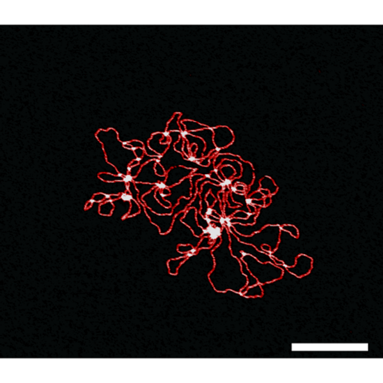
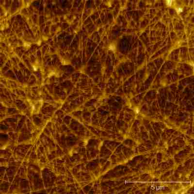
Verwicklungen Rasterkraftmikroskopische (AFM) Topographie-Aufnahme einer doppelsträngigen DNA (dsDNA) Die eingefärbten und verschlungenen, fadenartigen Strukturen sind die dsDNA-Fragmente. Der Hintergrund ist der frisch gespaltene Glimmer, an den die DNA-Fragmente adsorbiert wurden. Maßstabsbalken, 180 nm. Selen Manioglu PhD Student ETH Zürich/D-BSSE, Biophysics Lab
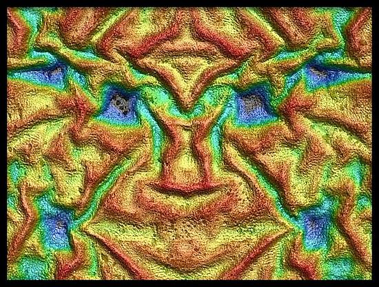
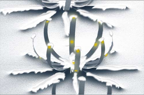
Weihnachtsstern Oberflächen-Topologie einer Entblendungsfolie, die für Beleuchtungslösungen verwendet wird. Die Charakterisierung wurde mit einem konfokalen Laser-Scanning-Mikroskop durchgeführt, und Teile des sich wiederholenden Musters wurden neu eingefärbt. Das Bild ist das Ergebnis einer Zusammenarbeit zwischen CSEM Center Muttenz und INKA, FHNW.Tamara Aderneuer SNI PhD Student Micro-Nano Optics, CSEM Muttenz


Nano Image Award 2019
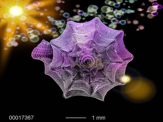
Lepicythara - Not really Nano but still very small and extremly attractive: a tiny snail from the genus Neogastropoda Daniel Mathys, Nano Imaging Lab, Swiss Nanoscience Institute, University of Basel


Nano Image Award 2018
Artificial crystals in two dimensions - Illustration of the periodic potential structure that forms when a single layer of carbon atoms (Graphene) is combined with two layers of Boron Nitride, one on top, one at the bottom, at different angles. Effects of such artificial crystal structures can be found in electronic devices fabricated in the Nano-electronics group at the University of Basel.- Andreas Baumgartner Department of Physics, University of Basel


Nano Image Award 2017


Nano Image Award 2016
Marietta Batzer, Dominik Rohner (Physics Department, University of Basel) Winter landscape. Diamond surface after etching with a plasma (rectangular paddles can be broken out and used as samples)


Nano Image Award 2015
Gulibusitan Abulizi: A real-color optical microscope image of an hexagonal boron nitride flake on a silicon oxide substrate The observed optical colors are due to interference effect, which can be used to determine the hexagonal boron nitride (hBN) flake thickness. Here, the observed color progresses from violet to blue, to green, to yellow, to orange, and to red, while the hBN flake thickness increases.


Nano Image Award 2014
Graphene Mosaic, Kishan Thodkar (University of Basel) The image was taken after the Chemical Vapour Deposition process of graphene on copper foil. After the growth, the foil was heated to 200°C for a minute to optically visualize regions of copper foil uncovered by graphene.
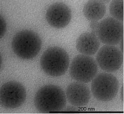
Virus-imprinted nanoparticles, Patrick Shahgaldian (FHNW), colorised by Martin Oeggerli (micronaut.ch). It is a color SEM micrograph of our virus-imprinted nanoparticles
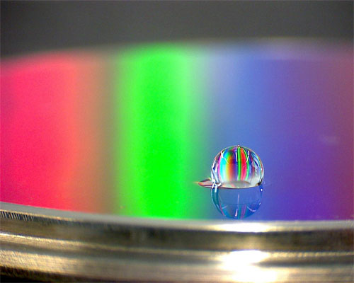
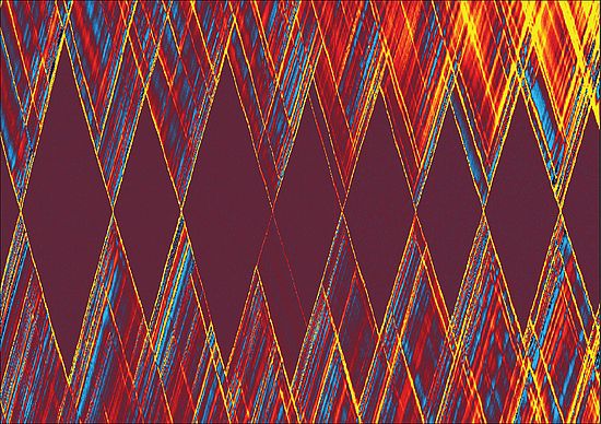
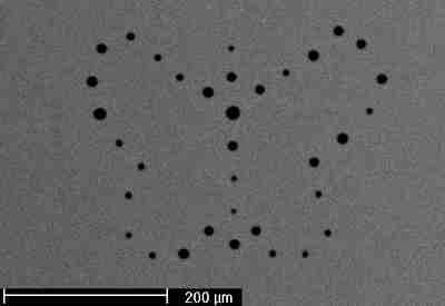
We caught the rainbow, Celestino Padeste (PSI) Water contact angle measurement on a nanostructured nickel master (5 cm in diameter) functionalized with an anti-sticking coating. The structured area consists of an array of pillars of 300 nm diameter with 600 nm period. (Collaboration FHNW/PSI/EULITHA/Applied Microswiss)


Nano Image Award 2010


Nano Image Award 2010
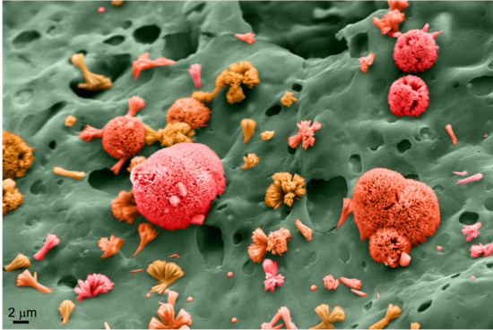
Wang Li, CSEM SEM images of the controlled positioning of Silver nanoparticles, which form nanoflowers and nanoleaves.
Markus Weiss Dark Field Image of sample that consists of a Carbon Nanotube Josephson Junction in an engineered electromagnetic environment.
Barbara Rothen, Uni Bern (Gruppe Gehr) Fluoreszenzmarkierte Liposomen (rot) mit einem Nanopolystyrolpartikel (gruen) innerhalb der Liposomen.
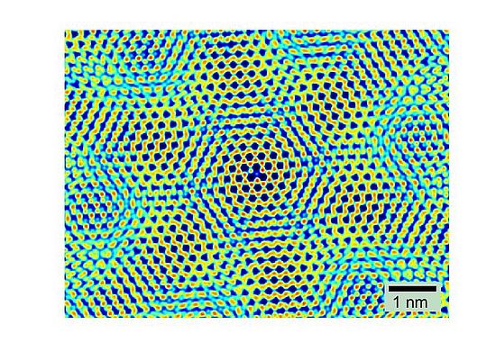
Enrico Gnecco "Lateral force map of the superstructure formed by an ultrathin KBr film deposited on NaCl" The frame size is 10 nm and the image was published in Phys. Rev. B 78 (2008) 045432 (authors: S. Maier, E. Gnecco, A. Baratoff, R. Bennewitz, and E. Meyer)
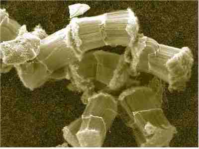
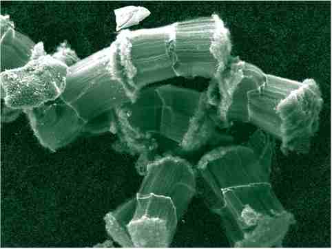
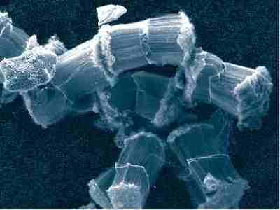
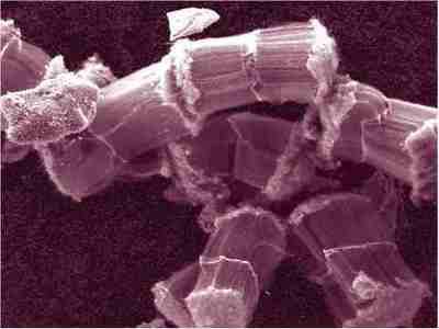
Christian Held SEM picture of tungstenoxide crystals on EPOXY glue. While examine the tungsten etched AFM/STM tips these nice structures were found. I admit not really nano, but still very nice.
Fabian Itel A fluorescence light microscope picture of a fluorescently labelled polymer-lipid mixtur monolayer.
André Kaufmann Die Bilder zeigen Felder von Nanotürmen mit einem Durchmesser von 170 nm und einer Höhe von 250 nm. Die Türme selber bestehen aus SiO2 (oberer Teil) und Si (unterer Teil) wobei sich die Grenzfläche auf einer Höhe von 60 nm befindet. Die Felder wurden gezielt mit einem SFM manipuliert um gewisse Strukturen abbilden zu können. Das Bild wurde im Anschluss an die Manipulation mit derselben Technik aufgenommen. Um die geschriebenen Strukturen sehen zu können, sollte man die Bilder ein wenig aus der Ferne betrachten. PS: Nebst PSI, SNI und IU (seinerzeit für meine Freundin geschrieben) hätte ich auch noch NCCR und LMN im Angebot.
André Kaufmann Die Bilder zeigen Felder von Nanotürmen mit einem Durchmesser von 170 nm und einer Höhe von 250 nm. Die Türme selber bestehen aus SiO2 (oberer Teil) und Si (unterer Teil) wobei sich die Grenzfläche auf einer Höhe von 60 nm befindet. Die Felder wurden gezielt mit einem SFM manipuliert um gewisse Strukturen abbilden zu können. Das Bild wurde im Anschluss an die Manipulation mit derselben Technik aufgenommen. Um die geschriebenen Strukturen sehen zu können, sollte man die Bilder ein wenig aus der Ferne betrachten. PS: Nebst PSI, SNI und IU (seinerzeit für meine Freundin geschrieben) hätte ich auch noch NCCR und LMN im Angebot.
André Kaufmann Die Bilder zeigen Felder von Nanotürmen mit einem Durchmesser von 170 nm und einer Höhe von 250 nm. Die Türme selber bestehen aus SiO2 (oberer Teil) und Si (unterer Teil) wobei sich die Grenzfläche auf einer Höhe von 60 nm befindet. Die Felder wurden gezielt mit einem SFM manipuliert um gewisse Strukturen abbilden zu können. Das Bild wurde im Anschluss an die Manipulation mit derselben Technik aufgenommen. Um die geschriebenen Strukturen sehen zu können, sollte man die Bilder ein wenig aus der Ferne betrachten. PS: Nebst PSI, SNI und IU (seinerzeit für meine Freundin geschrieben) hätte ich auch noch NCCR und LMN im Angebot.
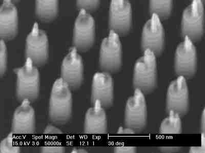
Mona Klein, CSEM "Waferscale-production of Bienenwachskerzen - just in time for christmas" Also Si pillars, etched with a modified procedure. The "flame" is due to residues of the polystyrene beads which where used to pattern the SiOx hard mask.
Mona Klein, CSEM "Waferscale-production of Bienenwachskerzen - just in time for christmas" Also Si pillars, etched with a modified procedure. The "flame" is due to residues of the polystyrene beads which where used to pattern the SiOx hard mask.
Mona Klein, CSEM Si pillars etched with a Bosch-like process using a SiOx mask patterned by self-assembled polystyrene beads stick their heads together due to charging in the SEM.
Andrea Lehmann, Uni Bern (Gruppe Gehr) Makrophagen (weiss, transparent, markiert ist das Aktin-Zytoskelett) mit intrazellulaeren Eisenplatin-Nanopartikeln (rot, fluoreszenzmarkierte Huelle).
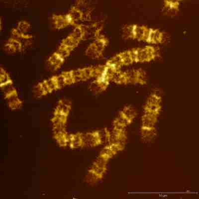
Marko Loparic Individual female chromosomes (from 6th to 13th chromosomes) isolated from blood and imaged with the AFM. Single GTG bands (chromatin condensates as bright bands) are detected without additional staining. Moreover, nanometer substructures of single chromosomes (hairy edges) are clearly resolved. Chromosomes are isolated in the group of Dr. Kathrin Hoffmann (University Hospital, Charité Berlin).
Marko Loparic Surface of the native cartilage imaged in quasi physiological conditions (PBS buffer) without staining or fixation. Collagen network is clearly resolved as rod like structures surrounded by aggregations of the proteoglycans.
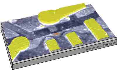
Nicholas Minder Scanning electron micrograph of a hybrid graphene device, which was fabricated during my master's thesis in the group of Christian Schönenberger (supervisor: Jelena Trbovic). The device consists of ferromagnetic (Cobalt, yellow) and superconducting electrodes (Aluminium, red) over mechanically exfoliated graphene (blue) on a 300nm SiO2/Si wafer (gray). The electrodes were fabricated by electron beam lithography and thermal evaporation.

Jérôme Wiss Picture taken with STM at room temperature. It shows a hexagonal assembly of a porphyrin (called TV151) on Ag111. The picture has dimensions of 14.8nm*14.8nm. The pores are filled also with TV151 that is probably rotating in the pores
Ana-Maria Popa Open_sesam is the in-situu monitoring by AFM in liquid media of the conformation change of a responsive polymer covalently grafted to a nanoporous surface upon a temperature sweep. Nano_english gardens is an SEM image of a micro-nanostructured surface fabricated by block-copolymer assisted lithography.


