Nano structures
Dimensions


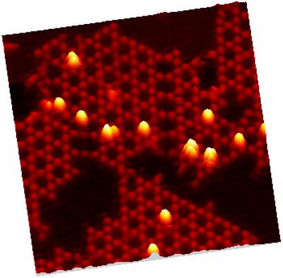
Surfaces in atomic resolution
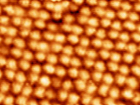
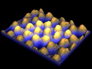
Cu-TBPP molecules on Cu(100) Size: 8.0 x 8.0 nm (Picture: C. Loppacher) Non-contact AFM / UHV Microscope, Group of Prof. E. Meyer
Cu-TBPP molecules on Cu(100) Size: 8.0 x 8.0 nm (Picture: C. Loppacher) Non-contact AFM / UHV Microscope, Group of Prof. E. Meyer See also: PRL, Vol. 90(6) (2003)
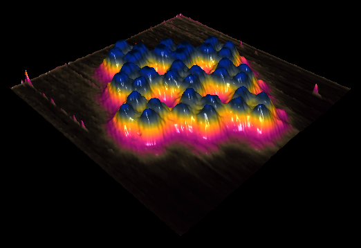
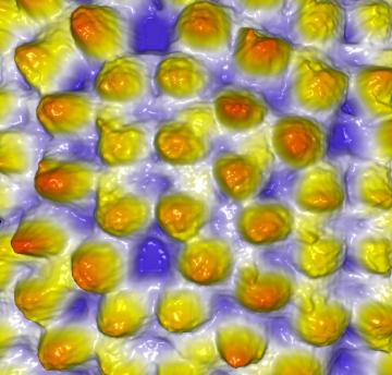
Cu-TBPP molecules on Cu(100) Size: 8.0 x 8.0 nm (Picture: C. Loppacher) Non-contact AFM / UHV Microscope, Group of Prof. E. Meyer See also: PRL, Vol. 90(6) (2003)

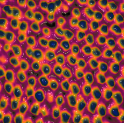
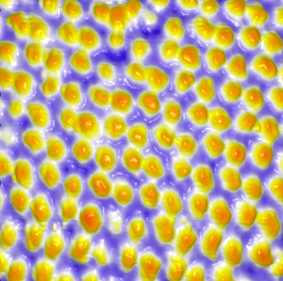
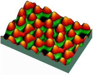
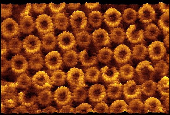
Monolayer of DMP (Monoporphyrin) on Ag(100) Size 12.2 x 9.1 nm, STM / Nanolab, Group Leader: Dr. T. Jung See also: Angew. Chem. 2004, 116
Monolayer of DMP (Monoporphyrin) on Ag(100) Size 12.2 x 9.1 nm, STM / Nanolab, Group Leader: Dr. T. Jung See also: Angew. Chem. 2004, 116
Monolayer of DMP (Monoporphyrin) on Ag(100) Size 12.2 x 9.1 nm, STM / Nanolab, Group Leader: Dr. T. Jung See also: Angew. Chem. 2004, 116
Monolayer of DMP (Monoporphyrin) on Ag(100) Size 12.2 x 9.1 nm, STM / Nanolab, Group Leader: Dr. T. Jung See also: Angew. Chem. 2004, 116
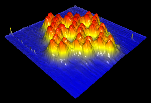
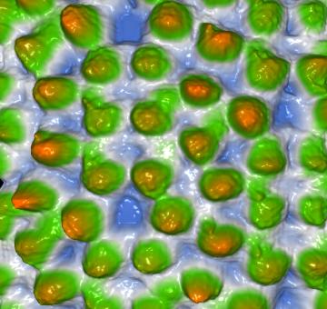
Monolayer of DMP (Monoporphyrin) on Ag(100) Size 12.2 x 9.1 nm, STM / Nanolab, Group Leader: Dr. T. Jung See also: Angew. Chem. 2004, 116
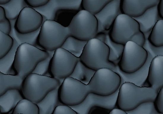
NaCl film grown on Cu(111) Size 9 x 9 nm, Picture: R.Bennewitz Non-contact AFM / UHV Microscope, Group of Prof. E. Meyer See also: Phys. Rev. B, 62, 2074, (2000)
NaCl film grown on Cu(111) Size 9 x 9 nm, Picture: R.Bennewitz Non-contact AFM / UHV Microscope, Group of Prof. E. Meyer See also: Phys. Rev. B, 62, 2074, (2000)
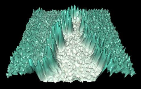
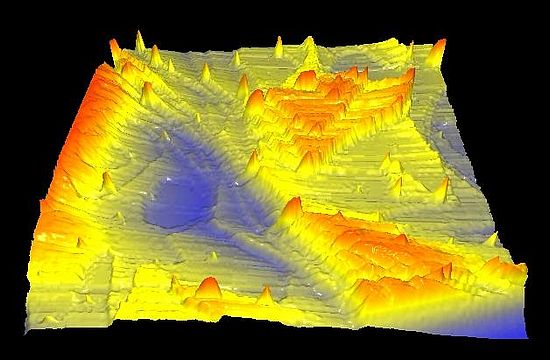
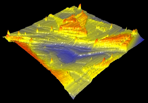
Silicon surface, Si(111) 7x7 Size: 5.00 x 5.00 nm, Picture: M. Lantz Non-contact low temperature AFM, Group of Prof. H. Hug See also: Phys. Rev. Lett., 84, 2642, 2000
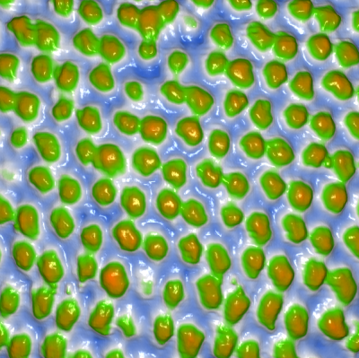
Silicon surface, Si(111) 7x7 Size: 5.00 x 5.00 nm, Picture: M. Lantz Non-contact low temperature AFM, Group of Prof. H. Hug See also: Phys. Rev. Lett., 84, 2642, 2000


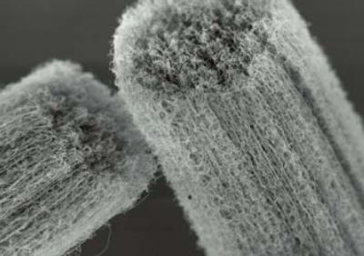
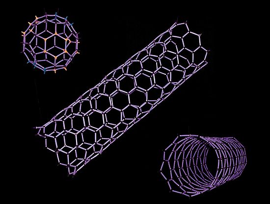
Carbon nanotubes
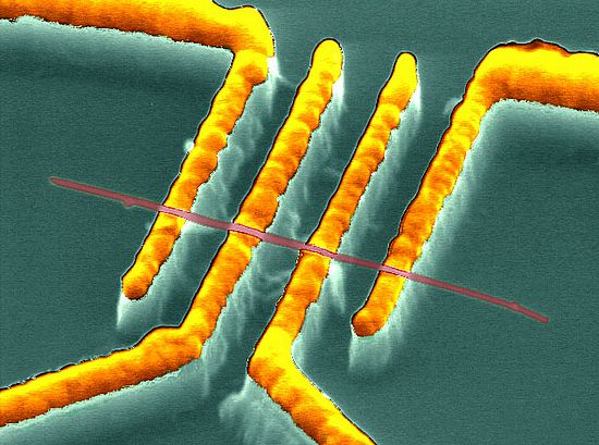
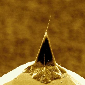
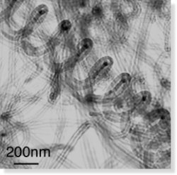
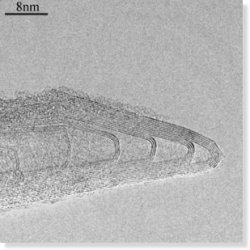
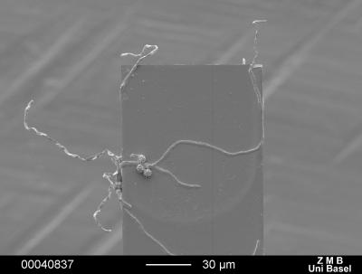
CNT on a cantilever tip Scanning electron-microscopy (SEM) image of a carbon nanotube (CNT) attached to a cantilever tip


Molecular machinery and devices
Molecular machinery and devices (Foto: IBM) (Images provided by R. Schlittler, IBM Zurich Research Laboratory, © IBM) See also: Module 1 – Nanobiology
Molecular machinery and devices (Foto: IBM) (Images provided by R. Schlittler, IBM Zurich Research Laboratory, © IBM) See also: Module 1 – Nanobiology
Molecular machinery and devices (Foto: IBM) (Images provided by R. Schlittler, IBM Zurich Research Laboratory, © IBM) See also: Module 1 – Nanobiology


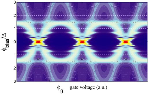
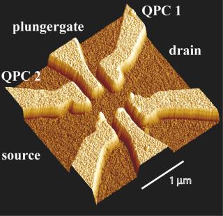
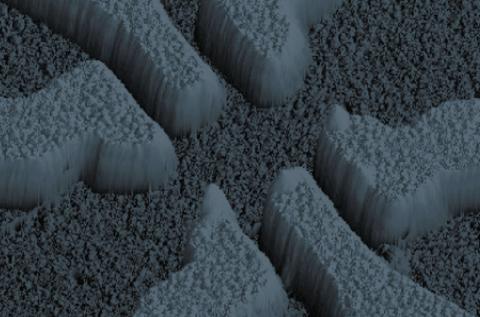
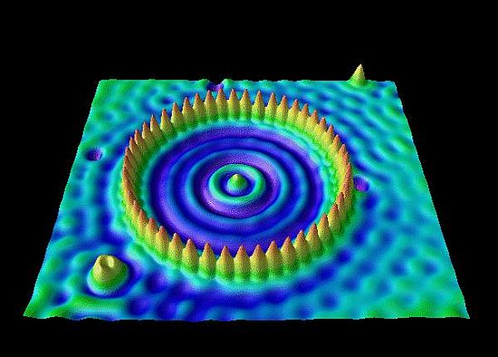
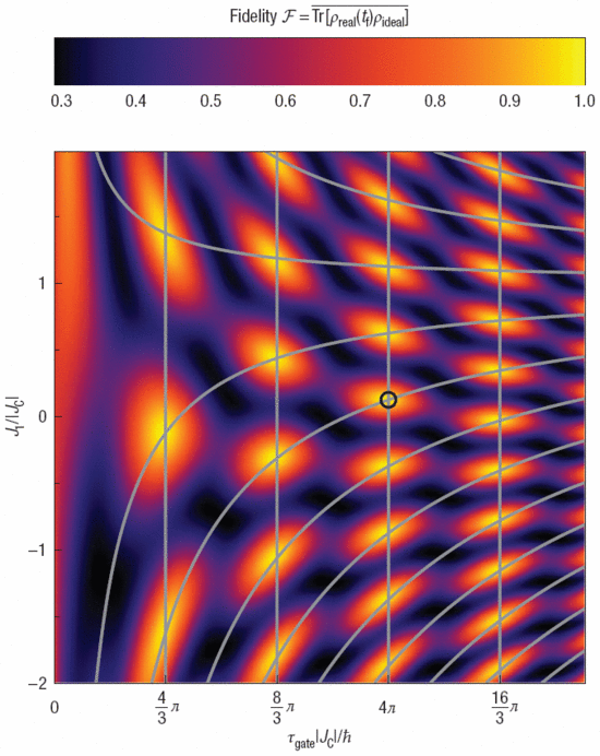
Quantum mechanical systems


Various
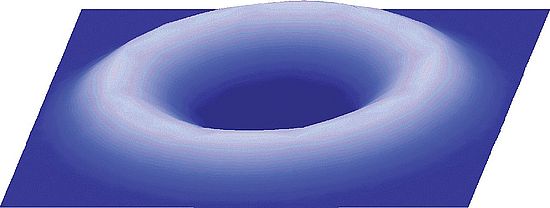
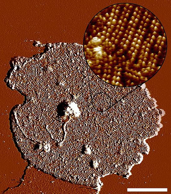
Asymmetric unit membrane (AUM) Imaging of the native asymmetric unit membrane (AUM) by contact mode scanning force microscopy (CMSFM) SFM reconstruction based on averaging over 100 plaque particles each for the luminal and cytoplasmic face of the asymmetric unit membrane (AUM) of urine bladder epithelium. The luminal side (upper left half in orange) of particles protrudes about 6.5nm relative to the lipid bilayer and the cytoplasmic face (lower right half in blue) only 0.5nm, hence the name "asymmetric unit membrane". Averages are based on contact mode SFM imaging in buffer solution. These particles form 2D crystalline plaques in situ. Center to center distance: 16nm
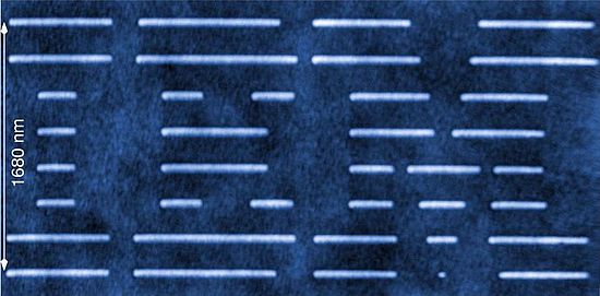
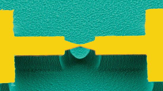
Direct Stencil Type Lithography Copper lines with a width of 40 nm fabricated on a silicon wafer surface by the stenciling technique nanonews January 2006

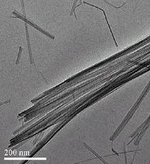
Inorganic Nanowires TEM image of Cu(OH)2 nanoribbons synthesized with addition of ammonia nanonews January 2006
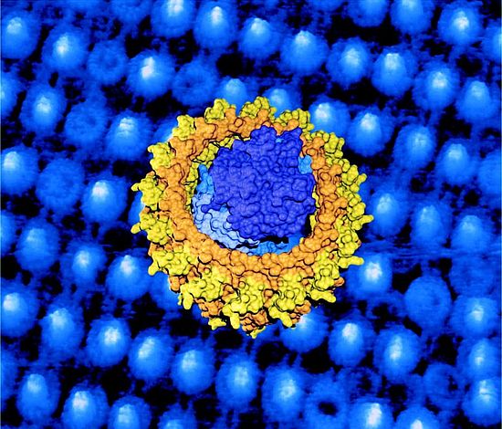
model of the light-harvesting 1-reaction center (RC-LH1) complex (photo: Fotiadis et al., front cover from Journal of Biological Chemistry, January 16th, 2004) Journal of Biological Chemistry, January 16th, 2004
Native disk membranes isolated from mice TEM image of Cu(OH)2 nanoribbons synthesized with addition of ammonia nanonews January 2006

Fibroblasts SFM imaging of cultured fibroblasts SFM imaging of rat-2 fibroblasts under optimal culture conditions. Confluent cells exhibiting their actin stress fiber network tightly adhering to the cytoplasmic face of the plasma membrane are depicted. (Picture: Tobias Reichlin)

Snapshot of a computer simulation reproducing the sliding motion of a tip on a surface on the atomic scale
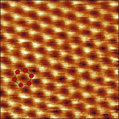
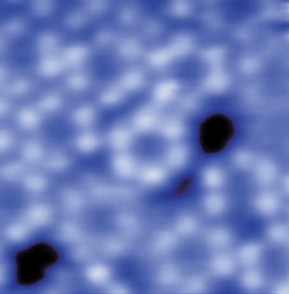
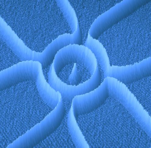
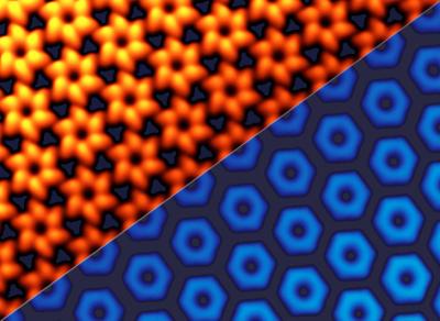
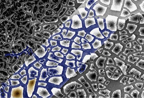
Submonolayer of DPDI Submonolayer of DPDI (4,9-diaminoperylene-quinone-3,10-diimine, a Perylen derivate) on Cu(111) surface. Under the influence of heat (300°C) a hexagonal network of Perylen-derivatives (DPDI) is formed. The emerging holes can be used to catch other molecules - here C60-molecules. (Picture: Meike Stöhr)