Crystalline structures made visible – the new TEM/STEM in the Nano Imaging Lab
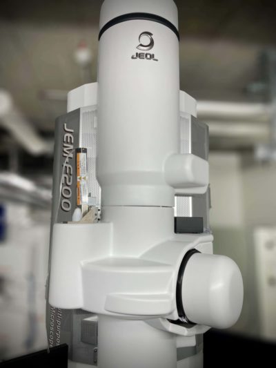
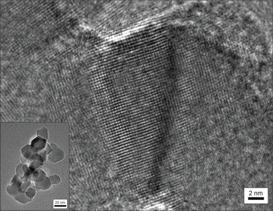


Our new scanning transmission electron microscope “JEOL JEM-F200 cFEG” has a cold field emission source and an acceleration voltage that is more than twice as high as the previous TEM in our laboratory. This, as well as the ability to scan the wafer-thin sample with the electron beam, make the STEM / TEM in combination with EDX a unique analysis device, which enables the imaging of the smallest crystal structures in condensed matter with atomic resolution and element analysis. A suitable sample preparation with the help of the FIB / SEM is added to the previous options, whereby TEM lamellae are produced.
Please contact Dr. Marcus Wyss marcus.wyss-at-unibas.ch if you wish to know more about our FIB and TEM services, or put a request on www.nanoimaging1.unibas.ch.