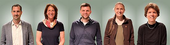
The team of the Nano Imaging Lab
The NI Lab team provides excellent service and can advise you on all scientific imaging matters:
Dr. Marcus Wyss, Susanne Erpel, Dr. Alexander Vogel, Evi Bieler, Dr. Monica Schönenberger
Dr. Marcus Wyss

Dr. Marcus Wyss studied Nanosciences at the University of Basel and received his doctorate in 2018 in the field of magnetic imaging techniques with a focus on nanometer sensor technology. After completing his studies, he conducted research into the development of a new design for sensors for the next generation of measuring SPM tips. He is the contact person for questions regarding the use of the focused ion beam microscope as well as the imaging, analysis, milling, and structuring of samples down to the nanometer range. He is interested in all scientific questions as well as the planning and implementation of challenging new research projects. He is also a dedicated teacher who knows how to convey science in a simple and pragmatic way to ensure knowledge transfer. This allows him to fully share his enthusiasm for research and development in the fields of nanometer sensors, quantum computing and nanofabrication.
Contact
Head of Nano Imaging Lab (100%) – Kragenbau, Room 0053
Swiss Nanoscience Institute (SNI) – Nano Imaging
Universität Basel
Pharmazentrum
Klingelbergstrasse 50
CH-4056 Basel
Phone: +41 61 207 65 26
Mail: marcus.wyss-at-unibas.ch
Dr. Monica Schönenberger

studied pharmacy in Basel and gained experience of atomic force microscopy during her doctorate at Hoffmann-La Roche under the guidance of Professor Hans-Joachim Güntherodt. After completing her doctorate, she worked as a project manager at Mepha AG before joining Professor Ernst Meyer’s group in the Department of Physics in 2006. After a year at Nanosurf, she then took on responsibility for the SNI’s new Nanotech Service Lab in 2010. Over the last few years, Dr. Schönenberger has developed a flexible, professional service unit for atomic force microscopy. She also teaches master’s and doctoral students to use the various scanning probe microscopes and enjoys getting involved in exciting new research projects.
Contact
Application scientist AFM/LSM (50%) – Kragenbau, Room 0055
Swiss Nanoscience Institute (SNI) – Nano Imaging
University of Basel
Pharmazentrum
Klingelbergstrasse 50
CH-4056 Basel
Phone: +41 61 207 14 05
Dr. Alexander Vogel

Dr. Alexander Vogel studied physics at ETH Zurich and completed his Master of Science in Physics in 2017. After a 6-month internship at ABB Semiconductors in Lenzburg, he studied the properties of ferroelectric thin-film layers as a doctoral student and post-doc at the Electron Microscopy Center of Empa Dübendorf and the Laboratory for Multifunctional Ferroic Materials of the ETH Zurich. During his research work, he specialized in transmission electron microscopy and in particular was engaged to various methods of atomically-resolved HAADF-STEM, STEM-EELS and Differential Phase Contrast (DPC)-STEM. At the Nano Imaging Lab he can now further expand his well-founded specialist knowledge and use it for new and interesting multi-disciplinary tasks.
Contact
Microscopy expert TEM/FIB & researcher (100%) – Kragenbau, Room 0053
Swiss Nanoscience Institute (SNI) – Nano Imaging
University of Basel
Pharmazentrum
Klingelbergstrasse 50
CH-4056 Basel
Phone: +41 61 207 14 04
Evi Bieler

trained as an academic/technical assistant with Professor Guggenheim in the scanning electron microscopy lab (SEM) and also studied English and German. She is part of the team since 2007 and mainly responsible for SEM analyses. She specializes in cryo-scanning electron microscopy, which she helped to develop in collaboration with industrial partners. She is also a valued source of information on all other matters relating to scanning electron microscopy, focusing not only on detailed imaging, but also using EDX (energy-dispersive X-ray microanalysis) to analyze the chemical composition of compounds, for example. Evi Bieler is fascinated by the possibilities offered by SEM and knows just how to convey this enthusiasm to students and clients. She is involved in the NI Lab’s PR work and helps to show children and visitors just how thrilling the micro world can be.
Contact
EM Technician SEM/TEM (60%) – Kragenbau, Room 0055
Swiss Nanoscience Institute (SNI) – Nano Imaging
University of Basel
Pharmazentrum
Klingelbergstrasse 50
CH-4056 Basel
Phone: +41 61 207 14 08
Mail: evi.bieler-at-unibas.ch
Susanne Erpel

trained as a biology/technical assistant and studied technical biology. She began to work with electron microscopy while completing her undergraduate dissertation. After completing her studies, she spent five years in charge of the microscopy service at the University of California, San Francisco. During this time, she performed all transmission electron microscopy (TEM) imaging for the university’s research associates and helped them to interpret the data obtained. After taking time off to have a family, Susanne Erpel moved to C-CINA in 2014 and joined the NI Lab in March 2016. She works largely with SEM analyses – particularly for the life sciences – which feed her fascination with making the invisible visible.
Contact
EM Technician SEM/TEM (80%) – Kragenbau, Room 0055
Swiss Nanoscience Institute (SNI) – Nano Imaging
University of Basel
Pharmazentrum
Klingelbergstrasse 50
CH-4056 Basel
Phone: +41 61 207 14 06