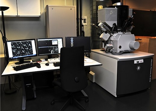
SEM – FEI Helios Nano Lab 650
Technical specifications

- High Resolution Field Emission (Schottky) Scanning Microscope (Dual Beam)
- Resolution of the electron beam:
– 0.8 nm at 15 kV
– 1.5 nm at 200 V - Resolution of the ion beam:
– 4.0 nm at 30 kV using preferred statistical method
– 2.5 nm at 30 kV using selective edge method - Maximum sample size: 150 mm in diameter, 55 mm in height
- Maximum sample weight: 500 g (incl. sample holder)
Detectors and micro analysis
- Elstar in-lens SE detector (TLD-SE)
- Elstar in-lens BSE detector (TLD-BSE)
- Everhart-Thornley SE detector (ETD)
- Energy Dispersive X-Ray Spectroscopy (EDX), Genesis & Team software
Typical applications and accessories
- Imaging, analysis, milling, patterning of specimens down to the nanoscale
- TEM lift out / TEM lamella
- Nanofabrication and micromanipulation
- Multiple gas injection system for Pt-, W-, C-, Co- and H20- deposition
- Correlative Microscopy (LM – SEM)
- 3-axis and Rotip Kleindiek micromanipulator
- Lift Out Shuttle from Kleindiek
- Eucentric five Axis Table from Kleindiek
Location
Pharmazentrum, U1007
